Turn-On Switching Loss of An A
Figure 1 shows a simplified buck converter with asynchronous rectification based on the MAX1744/5 controller IC. Due to the turn-off nature of the diode, turn-on switching loss of the main switch (Q1) depends on the switching frequency, the trace inductance of the input loop (consisting of C1, Q1 and D1), the gate charge (Miller capacitance) of the main switching MOSFET, and the drive capability of the control IC. This application note will provide detailed analysis of turn-on switching loss and the criteria for selecting the switching P-channel MOSFET.
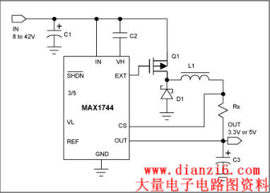
Figure 1. Typical asynchronous buck converter based on the MAX1744 control IC.
Figure 2 shows the typical waveforms of Q1. During the turn on of Q1, the gate voltage, Vg, charges up first. Once it reaches the threshold voltage, Q1 turns on and the drain to source voltage of Q1, Vds, decreases. Meanwhile, the drain current of Q1 and Id increases. Turn-on cross-conduction loss occurs during this time interval. Three situations are considered, depending on the trace inductance, Ltr:
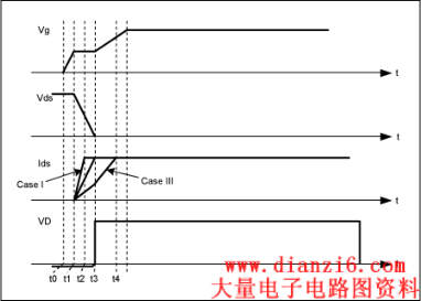
Figure 2. Typical switching waveforms of Q1 and the diode voltage, VD.
Case I: The trace inductance is relatively small. The drain current reaches the output current, Io, before the drain to source voltage reaches zero.
Case II: The trace inductance has a critical value such that the drain current reaches zero at the same time when the drain to source voltage is zero.
Case III: The trace inductance is relatively large so that the drain current does not reach the output current after the drain to source voltage becomes zero.
In the above three cases, Case I has the highest switching loss, while Case III has the lowest switching loss, as shown in Figure 2. Case I produces the highest overlap between Ids and Vds. Before we start the analysis, the time needed to discharge the Miller capacitance of Q1 is given by,
where Qg is the Miller charge, Rg is the gate resistance of Q1, Rd is the on-resistance of the MOSFET driver, Vd is the supply voltage of the driver and VT is the threshold voltage of Q1.
The equivalent circuit for turn on transition is given in Figure 3, where Cgd is the Miller capacitance, the voltage-controlled voltage source represents the discharge of the drain to source voltage, Vds.
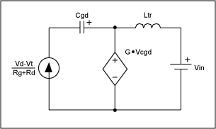
Figure 3. Equivalent circuit for turn-on switching transition.
The time period for the drain current, Id, charging up to the output current, Io, is given by,
From Eq. (1) and Eq. (2), we have,
For given Io, and Vin, there are a few ways to make ΔT1 ≥ ΔT. First, choose Q1 with less Miller charge, less gate resistance and less gate threshold voltage. Second, increase the supply voltage of the MOSFET driver, and third increase the trace inductance. The third choice is not encouraged due to possible oscillation after the turn-on switching transition. This is because after the switching transition is finished, the energy stored in the trace inductor will oscillate with the junction capacitance of the diode to dissipate the energy. Therefore, a MOSFET driver with higher supply voltage and lower on-resistance will minimize the turn-on conduction loss. On the other hand, once the layout and driver is fixed, choosing a MOSFET with less Miller charge and lower threshold voltage will minimize the turn on cross conduction loss.
It should be pointed out that the turn-on switching loss includes two parts: one is the above-mentioned turn-on cross conduction loss and the other is the discharging loss of the output capacitance of Q1. The latter is a fixed amount of loss and has nothing to do with the drive capability and layout parameters. Using the parameters obtained from the MAX1744 EV kit yields the ratio of ΔT1/ΔT equal to 0.4, which is in the Case I category, the Ltr is assumed 15nH, Qg = 10nC, Rg = 2Ω, and VT = 3V. If we switch the Q1 from NDS9407 (Qg = supply number, Rg = supply number) to Si9407, a FET with Qg = 3nC and Rg = 1Ω, the ratio ΔT1/ΔT is equal to 0.77. Figure 3 shows the comparison of the efficiencies of using NDS9407 and Si9407 on the same EV kit. It is evident from Figure 2 that the efficiency is improved about 1% at all load conditions. If Rd is halved, ΔT1/ΔT is then equal to 1.03, which is preferred in terms of switching loss. For high input voltage applications (Vin > supply a number), which are common with the MAX1744, turn-on cross conduction loss is more pronounced than that of the discharge loss of the output capacitance of Q1.
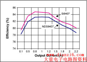
Figure 4a. Efficiency comparison at 12V input and 3.3V output.
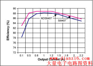
Figure 4b. Efficiency comparison at 12V input and 5V output.
如果觉得
Turn-On Switching Loss of An A这篇文章不错,可以推荐给朋友分享哦。
 温馨提示; 本站的资料全部免费下载,为方便下次找到本站记得将本站加入收藏夹哦,牢记网址http://www.dianzi6.com