热门关键字:
| 电路设计 单片机学习 PCB设计 电子制作 电工基础 电路基础 电子电路图 电脑技术 维修教程 手机数码 家电维修 电力技术 电气技术 |
| 电子基础 arm嵌入式 集成电路 模拟电子 电源管理 显示光电 楼宇控制 安防监控 控制电路 音响功放 单元电路 电子下载 维修资料下载 |
Designing the DS2726 to Protect Li+ Batteries During a Reverse Charger Event
Abstract: This application presents simple design modifications that will allow the Li+ protector to withstand negative voltages and protect the battery during a reverse charger event.
A reverse charger connection can defeat the DS2726 Li+ protector circuit. Certain device pins are sensitive to negative voltages and will cause the IC to behave erratically. The DS2726's high-side p-channel FETs will turn off, but some pins on the DS2726 cannot withstand the resulting negative voltages. The article will discuss both adding Schottky diodes to clamp the voltage on these pins, and increasing the resistance on these pins to limit the current/power dissipation. These simple design modifications will allow the DS2726 to survive a reverse charger event.
Refer to the schematic in Figure 1 for all component references.
PKP is the pin most exposed to the reverse charger's voltage. The typical application circuit already has a Schottky diode on this pin to prevent inductive kicks, caused by overcurrent events, from pulling the pin below ground. The only modification required is to increase the resistance on PKP, thus limiting the current through the Schottky diode.
A ten-cell stack will use a 42V charger.
A 60V Schottky will have a Vf = 0.45.
The voltage drop across RPKP is -42V - (-0.45V) = -41.55V
Assume that a 250mW resistor is used:
250mW = (-41.55V)²/RPKP
RPKP = 6.905kΩ
The next pin that will be exposed to the negative charge voltage is CC. Under normal operation CC will drive the charge-control FET's gate to the voltage on the PKP pin to turn off the FET. CC will drive ~ 10V below PKP to turn the FET on. Since PKP will be clamped at -0.45V, CC cannot turn the charge FET on. The charge-control FET is, moreover, only rated to a ±20V gate-to-source voltage. Therefore, if the varistor, V2, ties the charge-control FET's gate to source, this will protect the CC FET from being damaged. Without V2 the gate-to-source voltage would be ~ -42V, which exceeds the FET's rating.
The varistor will turn on at 16V, clamping the gate-to-source voltage.
The gate voltage of the CC FET will be -42V + 16V = -26V.
The voltage drop across the resistor on CC will be -26V - (-0.45V) = -25.55V.
Assume that a 250mW resistor is used:
250mW = (-25.55V)²/RCC
RCC = 1.857kΩ
The larger resistances on CC and PKP will cause the turn-on/turn-off time of the charge-control FET to increase. This will, in turn, cause the FET to be in the linear region for a longer period of time during turn-on. This condition should not, however, be a problem because the current is limited by the charger.
Even though the CC FET is off, its body diode will be on due to the negative voltage on PK+. This condition will put a negative voltage on SNS. Consequently, SNS is the last pin that needs to be clamped with a Schottky diode.
The voltage at the common drains of the protection FETs will be -42V + 0.6V = -41.4V.
The voltage on SNS will be clamped at -0.45V.
The voltage drop across the SNS resistor is -41.4V - (-0.45V) = -39.95V.
Assume that a 250mW resistor is used:
250mW = (-39.95V)²/RCC
RCC = 6.384kΩ
The comparator on the SNS pin will draw ~ 1µA:
1µA × 6.384kΩ = 6.384mV
This will introduce an error of ~ 6.4mV in the overcurrent trip points. If a higher-wattage resistor is used, then the resistor's value can be reduced which, in turn, will decrease this error.
Note: The time constant of the RC filter on SNS will change with the increased resistance. Consequently, the capacitor's value should be changed to maintain a similar time constant with the new resistor value. The time constant on SNS should match the time constant on RDOC and RSC. If the time constants on these pins do not match, then additional error will be introduced in the overcurrent trip point.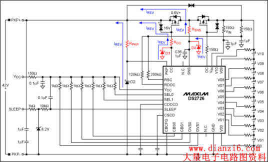
Figure 1. Modified typical application so the DS2726 passes a reverse charger connection.
The DS2726 Li+ battery protector can be modified to protect the batteries if a charger is connected in reverse. There are some design tradeoffs to consider, but none of them are critical to the overall operation of the protector. The calculations in this application note assume the power rating of the resistors to be 250mW. Using higher power resistors will allow the use of smaller resistance values. Smaller resistance values will reduce both the offset error in the overcurrent threshold and the delay seen in CC turn-on/turn-off times. Caution must still be taken to ensure that the constant-current limit of the Schottky diodes is not exceeded.
如果觉得 Designing the DS2726 to Protec这篇文章不错,可以推荐给朋友分享哦。 温馨提示; 本站的资料全部免费下载,为方便下次找到本站记得将本站加入收藏夹哦,牢记网址http://www.dianzi6.com
|
此页提供Designing the DS2726 to Protec高级电源管理,电源管理ic,电源管理软件, 电源管理参考。本站还有更多的电源管理相关资料分享。
Copyright© www.dianzi6.com Inc. All rights reserved 。 1 2 3 4 5 6 7 8 |
|