PCI Express板设计规则 (内部资料) 下载
- 文件类型:
- eda技术,EDA/PLD
- 文件大小:
- 842 KB
- 下载次数:
- [608次]
- 日期:
- 12-05
- 解压密码:
- www.dianzi6.com
- Tag:
- EDA/PLD,eda技术 PCI Express 规则 资料 设计
- 运行平台:
- txt/doc/word/ppt/pdf 等
- 星级:
-

-

正文:
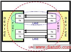
This document provides practical, common guidelines for incorporating PCI Express interconnect layouts onto Printed Circuit Boards (PCB) ranging from 4-layer desktop baseboard designs to 10-layer or more server baseboard designs. Guidelines and constraints in this document are intended for use on both baseboard and add-in card PCB designs. This includes interconnects between PCI Express devices located on the same baseboard (chip-to-chip routing) and interconnects between a PCI Express device located “down” on the baseboard and a device located “up” on an add-in card attached through a connector.
This document is intended to cover all major components of the physical interconnect including design guidelines for the PCB traces, vias and AC coupling capacitors, as well as add-in card edge-finger and connector considerations. The intent of the guidelines and examples is to help ensure that good high-speed signal design practices are used and that the timing/jitter and loss/attenuation budgets can also be met from end-to-end across the PCI Express interconnect.However, while general physical guidelines and suggestions are given, they may not necessarily guarantee adequate performance of the interconnect for all layouts and implementations.
Therefore, designers should consider modeling and simulation of the interconnect in order to
ensure compliance to all applicable specifications.
The document is composed of two main sections. The first section provides an overview of
general topology and interconnect guidelines. The second section concentrates on physical layout constraints where bulleted items at the beginning of a topic highlight important constraints, while the narrative that follows offers additional insight.
如果觉得《PCI Express板设计规则 (内部资料)》不错,可以推荐给好友哦。
- 下载

- 进入下载地址列表
 温馨提示; 本站的资料全部免费下载,为方便下次找到本站记得将本站加入收藏夹哦,牢记网址http://www.dianzi6.com