ADC中的ABC:理解ADC误差对系统性能的影响,The A
ADC中的ABC:理解ADC误差对系统性能的影响 The ABCs of ADCs: Understanding How ADC Errors Affect System Performance
Abstract: Many design engineers will encounter the subtleties in ADC specifications that often lead to less-than-desired system performance. This article explains how to select an ADC based on the system requirements and describes the various sources of error when making an ADC measurement.
Using a 12-bit-resolution analog-to-digital converter (ADC) does not necessarily mean your system will have 12-bit accuracy. Sometimes, much to the surprise and consternation of engineers, a data-acquisition system will exhibit much lower performance than expected. When this is discovered after the initial prototype run, a mad scramble for a higher-performance ADC ensues, and many hours are spent reworking the design as the deadline for preproduction builds fast approaches. What happened? What changed from the initial analysis? A thorough understanding of ADC specifications will reveal subtleties that often lead to less-than-desired performance. Understanding ADC specifications will also help you in selecting the right ADC for your application.
We start by establishing our overall system-performance requirements. Each component in the system will have an associated error; the goal is to keep the total error below a certain limit. Often the ADC is the key component in the signal path, so we must be careful to select a suitable device. For the ADC, let's assume that the conversion-rate, interface, power-supply, power-dissipation, input-range, and channel-count requirements are acceptable before we begin our evaluation of the overall system performance. Accuracy of the ADC is dependent on several key specs, which include integral nonlinearity error (INL), offset and gain errors, and the accuracy of the voltage reference, temperature effects, and AC performance. It is usually wise to begin the ADC analysis by reviewing the DC performance, because ADCs use a plethora of nonstandardized test conditions for the AC performance, making it easier to compare two ICs based on DC specifications. The DC performance will in general be better than the AC performance.
System Requirements
Two popular methods for determining the overall system error are the root-sum-square (RSS) method and the worst-case method. When using the RSS method, the error terms are individually squared, then added, and then the square root is taken. The RSS error budget is given by:

where EN represents the term for a particular circuit component or parameter. This method is most accurate when the all error terms are uncorrelated (which may or may not be the case). With worst-case error analysis, all error terms add. This method guarantees the error will never exceed a specified limit. Sinceit sets the limit of how bad the error can be, the actual error is always less than this value (often-times MUCH less).
The measured error is usually somewhere between the values given by the two methods, but is often closer to the RSS value. Note that depending on one's error budget, typical or worst-case values for the error terms can be used. The decision is based on many factors, including the standard deviation of the measurement value, the importance of that particular parameter, the size of the error in relation to other errors, etc. So there really aren't hard and fast rules that must be obeyed. For our analysis, we will use the worst-case method.
In this example, let's assume we need 0.1% or 10 bits of accuracy (1/210), so it makes sense to choose a converter with greater resolution than this. If we select a 12-bit converter, we can assume it will be adequate; but without reviewing the specifications, there is no guarantee of 12-bit performance (it may be better or worse). For example, a 12-bit ADC with 4LSBs of integral nonlinearity error can give only 10 bits of accuracy at best (assuming the offset and gain errors have been calibrated). A device with 0.5LSBs of INL can give 0.0122% error or 13 bits of accuracy (with gain and offset errors removed). To calculate best-case accuracy, divide the maximum INL error by 2N, where N is the number of bits. In our example, allowing 0.075% error (or 11 bits) for the ADC leaves 0.025% error for the remainder of the circuitry, which will include errors from the sensor, the associated front-end signal conditioning circuitry (op amps, multiplexers, etc.), and possibly digital-to-analog converters (DACs), PWM signals, or other analog-output signals in the signal path.
We assume that the overall system will have a total-error budget based on the summation of error terms for each circuit component in the signal path. Other assumptions we will make are that we are measuring a slow-changing, DC-type, bipolar input signal with a 1kHz bandwidth and that our operating temperature range is 0°C to 70°C with performance guaranteed from 0°C to 50°C.
DC Performance
Differential nonlinearity
Though not mentioned as a key parameter for an ADC, the differential nonlinearity (DNL) error is the first specification to observe. DNL reveals how far a code is from a neighboring code. The distance is measured as a change in input-voltage magnitude and then converted to LSBs (Figure 1). Note that INL is the integral of the DNL errors, which is why DNL is not included in our list of key parameters. The key for good performance for an ADC is the claim "no missing codes." This means that, as the input voltage is swept over its range, all output code combinations will appear at the converter output. A DNL error of <±1LSB guarantees no missing codes (Figure 1a). In Figures 1b, 1c, and 1d, three DNL error values are shown. With a DNL error of -0.5LSB (Figure 1b), the device is guaranteed to have no missing codes. With a value equal to -1LSB (Figure 1c), the device is not necessarily guaranteed to have no missing codes. Note that code 10 is missing. However, most ADCs that specify a maximum DNL error of +/-1 will specifically state whether the device has missing codes or not. Because the production-test limits are actually tighter than the data-sheet limits, no missing codes is usually guaranteed. With a DNL value greater than -1 (-1.5LSB in Figure 1d), the device has missing codes.
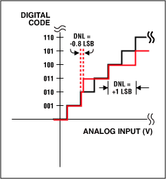
Figure 1a. DNL error: no missing codes.

Figure 1b. DNL error: no missing codes.
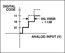
Figure 1c. DNL error: Code 10 is missing.
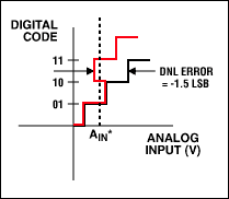
Figure 1d. DNL error: At AIN* the digital code can be one of three possible values. When the input voltage is swept, Code 10 will be missing.
When DNL-error values are offset (that is, -1LSB, +2LSB), the ADC transfer function is altered. Offset DNL values can still in theory have no missing codes. The key is having -1LSB as the low limit. Note that DNL is measured in one direction, usually going up the transfer function. The input-voltage level required to create the transition at code [N] is compared to that at code [N+1]. If the difference is 1LSB apart, the DNL error is zero. If it is greater than 1LSB, the DNL error is positive; if it is less than 1LSB, the DNL error is negative.
Having missing codes is not necessarily bad. If you need only 13 bits of resolution and you have a choice between a 16-bit ADC with a DNL specification < = +/-4LSB DNL (which is effectively 14 bits, no missing codes) that costs $5 and a 16-bit ADC with a DNL of < = +/-1LSB that costs $15, then buying the lower-grade version of the ADC will allow you to greatly reduce component cost and still meet your system requirements.
INL
INL is defined as the integral of the DNL errors, so good INL guarantees good DNL. The INL error tells how far away from the ideal transfer-function value the measured converter result is. Continuing with our example, an INL error of +/-2LSB in a 12-bit system means the maximum nonlinearity error may be off by 2/4096 or 0.05% (which is already about two-thirds of the allotted ADC error budget). Thus, a 1LSB (or better) part is required. With a +/-1LSB INL error, the accuracy is 0.0244%, which accounts for 32.5% of the allotted ADC error budget. With a specification of 0.5LSB, the accuracy is 0.012%, and this accounts for only about 16% (0.012%/0.075%) of our ADC error budget limit. Note that neither INL nor DNL errors can be calibrated or corrected easily.
Offset and Gain Errors
Offset and gain errors can easily be calibrated out using a microcontroller (µC) or a digital signal processor (DSP). With offset error, the measurement is simple when the converter allows bipolar input signals. In bipolar systems, offset error shifts the transfer function but does not reduce the number of available codes (Figure 2). There are two methodologies to zero out bipolar errors. In one, you shift the x and y axes of the transfer function so that the negative full-scale point aligns with the zero point of a unipolar system (Figure 3a). With this technique, you simply remove the offset error and then adjust for gain error by rotating the transfer function about the "new" zero point. The second technique entails using an iterative approach. First apply zero volts to the ADC input and perform a conversion; the conversion result represents the bipolar zero offset error. Then perform a gain adjustment by rotating the curve about the negative full-scale point (Figure 3b). Note that the transfer function has pivoted around point A, which moves the zero point away from the desired transfer function. Thus, a subsequent offset-error calibration may be required.
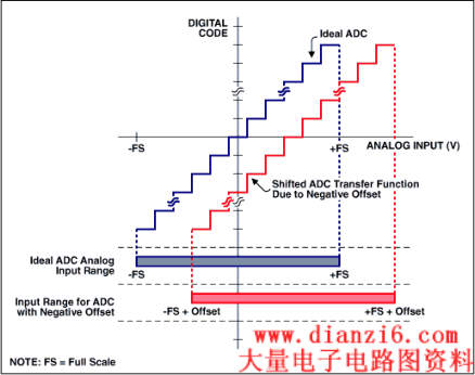
Figure 2. Bipolar offset error.
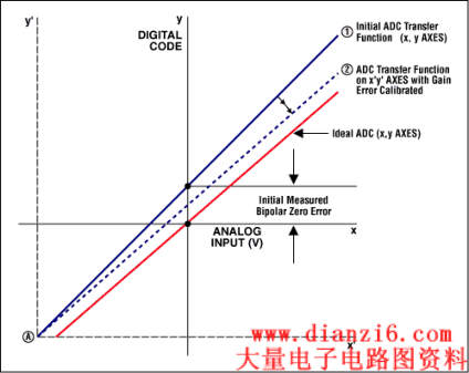
Figure 3a.
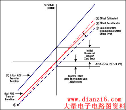
Figure 3b.
Figures 3a and 3b. Calibrating bipolar offset error. (Note: The stair-step transfer function has been replaced by a straight line, because this graph shows all codes and the step size is so small that the line appears to be linear.)
Unipolar systems are a little trickier. If the offset is positive, use the same methodology as that for bipolar supplies. The difference here is that you lose part of the ADC's range (see Figure 4). If the offset is negative, you cannot simply do a conversion and expect the result to represent the offset error. Below zero, the converter will just display zeros. Thus, with a negative offset error, you must increase the input voltage slowly to determine where the first ADC transition occurs. Here again you lose part of the ADC range.
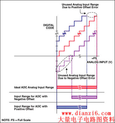
Figure 4. Unipolar offset error.
Returning to our example, two scenarios for offset error are given below:
- If the offset error is +8mV, with a 2.5V reference this corresponds to 13LSBs of error for a 12-bit ADC (8mV/[2.5V/4096)]. Though the resolution is still 12 bits, you must subtract 13 codes from each conversion result to compensate for the offset error. Note that the actual, measurable, full-scale value in this scenario is now 2.5V (4083/4096) = 2.492V. Any value above this will over-range the ADC. So, the dynamic range, or range of input values, for the ADC has been reduced. This is even more important for higher-resolution ADCs; 8mV represents 210LSBs at the 16-bit level (VREF = 2.5V).
- If the offset is -8mV (assuming a unipolar input), then small analog-input values near zero will not register when a conversion is performed until the analog input exceeds +8mV. This too reduces the dynamic range of the ADC.
Gain error is defined as the full-scale error minus the offset error (Figure 5). Full-scale error is measured at the last ADC transition on the transfer-function curve and compared against the ideal ADC transfer function. Gain error is easily corrected in software with a linear function y = (m1/m2)(x), where m1 is the slope of the ideal transfer function and m2 is the slope of the measured transfer function (Figure 5).
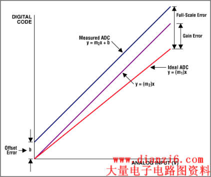
Figure 5. Offset, gain, and full-scale errors.
The gain-error specification may or may not include errors contributed by the ADC's voltage reference. In the electrical specifications, it is important to check the conditions to see how gain error is tested and to determine whether it is performed with an internal or external reference. Typically, the gain error is much worse when an on-chip reference is used. If the gain error were zero, when a conversion is performed the conversion result would begin to yield all ones (3FFh in our 12-bit example) when the full-scale analog input is applied (see Figure 6). As our converter is not ideal, you can initially end up with all ones in the conversion result when a voltage greater than full-scale is applied (negative gain error) or when a voltage less than full-scale is applied (positive gain error). Two ways to adjust for gain error are to either tweak the reference voltage such that at a specific reference-voltage value the output gives full-scale or use a linear correction curve in software to change the slope of the ADC transfer-function curve (a first-order linear equation or a lookup table can be used).
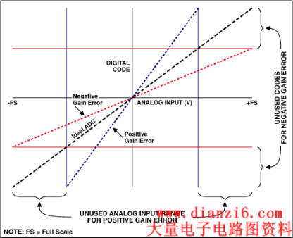
Figure 6. Gain error reduces dynamic range.
As with offset error, you lose dynamic range with gain error. For example, if a full-scale input voltage is applied and the code obtained is 4050 instead of the ideal 4096 (for a 12-bit converter), this is defined as negative gain error, and in this case the upper 46 codes will not be used. Similarly, if the full-scale code of 4096 appears with an input voltage less than full-scale, the ADC's dynamic range is again reduced (see Figure 6). Note that, with positive full-scale errors, you cannot calibrate beyond the point where the converter gives all ones in the conversion result.
The easiest way to handle offset and gain errors is to find an ADC with values low enough so that you don't have to calibrate. It's fairly easy to find 12-bit ADCs with offset and gain errors less than 4LSB.
Other Subtle Error Sources
Code-Edge Noise
Code-edge noise is the amount of noise that appears right at a code transition on the transfer function. It is often not specified in the data sheet. Even higher-resolution converters (16+ bits), where code-edge noise is much more prevalent due to the smaller LSB size, will often not specify code-edge noise. Sometimes, code-edge noise can be several LSBs. Conversions performed with the analog input right at the code edge can result in code flicker in the LSBs. Significant code-edge noise means that an average of samples must be taken to effectively remove this noise from the converter results. How many samples are needed? If the code-edge noise is 2/3LSB RMS, this equates to approximately 4LSB p-p. Sixteen samples will have to be taken to reduce the noise to 1LSB (the square root of the number of samples determines the improvement in performance).
The Reference
One of the biggest potential sources of errors in an ADC with an internal or external reference is the reference voltage. Often, if the reference is included on-chip, it is not specified adequately. To understand the source of the reference errors, it is important to look at three specs in particular: temperature drift, voltage noise, and load regulation.
Temperature Drift
Temperature drift is the most overlooked specification in the data sheet. As an example, note how temperature drift affects the performance of an ADC converter based on resolution (Figure 7). For a 12-bit converter to maintain accuracy over the extended temperature range (-40°C to +85°C), the drift must be a maximum of 4ppm/°C. Unfortunately, no ADC converter is available with this kind of on-chip-reference performance. If we relax the requirements, a 10-degree temperature excursion means the 12-bit ADC reference can drift no more than 25ppm/°C, which again is a fairly tight requirement for on-chip references. Prototyping frequently does not reveal the significance of this error, because parts are often from a similar lot and thus the test results do not take into account the extremes that occur in specs due to manufacturing-process variations.
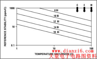
Figure 7. Voltage-reference-drift requirements relate to ADC resolution.
For some systems, the reference accuracy is not a big issue, as the temperature is held constant, eliminating the drift problem. Some systems use a ratiometric measurement, where the reference errors are removed because the same signal that excites the sensor is used as the reference voltage (Figure 8). Because the excitation source and reference move as one, drift errors are eliminated.

Figure 8. Ratiometric ADC conversion.
In other systems, calibration is performed often enough so that reference drift is effectively removed. In still other systems, absolute accuracy is not critical, but relative accuracy is. Therefore, the reference can drift slowly with time and the system will provide the desired accuracy.
Voltage Noise
Another important spec is voltage noise. It is often specified as either an RMS value or a peak-to-peak value. Convert the RMS value to a peak-to-peak value to evaluate its effect on performance. If a 2.5V reference has 500µV of peak-to-peak voltage noise at the output (or 83µV RMS), this noise represents 0.02% error or barely 12-bit performance, and this is before any of the converter errors are considered. Ideally, our reference-noise performance should be a small fraction of an LSB so as not to limit the ADC's performance. ADCs with on-chip references usually don't specify voltage noise, so the error is up to the user to determine. If you are not getting the performance you desire and are using an internal reference, try using a very good external reference to determine if the on-chip reference is in fact the culprit.
Load Regulation
The final spec is reference load regulation. Often the voltage reference used for an ADC has ample current to drive other devices, so it is used by other ICs. The current drawn by those other components will affect the voltage reference, which means that as more current is drawn the reference voltage will droop. If the devices using the reference are turning on and off intermittently, the result will be a reference voltage that moves up and down. A 0.55µV/µA reference-load-regulation specification for a 2.5V reference means that, if other devices draw 800µA, the reference voltage will change up to 440µV, which is .0176% (440µV/2.5V) or almost 20% of the available error margin.
Other Temperature Effects
Continuing with the topic of temperature, two specifications that are often given little attention are offset drift and gain drift. These specs are usually given as typical numbers only, leaving it up to the users to determine if the specification is good enough for their system requirements. Offset- and gain-drift values can be compensated in a couple of different ways. One way is to fully characterize the offset and gain drift, and provide a lookup table in memory to adjust the values as temperature changes. This, however, is a cumbersome process, as each ADC must be compensated individually and the compensation process is a time-consuming effort. The second method is to perform calibrations when a significant temperature change has occurred.
With systems that do a one-time temperature calibration, it's important to pay heed to the drift specs. If the initial offset is calibrated and the temperature moves, there will be an error introduced due to the drift term that can negate the effects of the calibration. For example, assume a reading is done at temperature X. Some time later, the temperature has changed 10°C and the exact same measurement is taken. These two readings can give different results, calling into question the repeatability and thus the reliability of the system.
There is a good reason why manufacturers do not give maximum limits: This increases the cost. Drift testing requires special boards, and an extra step must be added to the test flow (which equates to an additional manufacturing cost) to make sure the parts do not exceed the maximum-drift limit.
Gain drift is more of an issue, particularly for devices tested with an internal reference. In this case, the reference drift can be included in the gain-drift parameter. For an external reference, the IC's gain drift is typically fairly small, like 0.8ppm/°C. Thus, a +/-10 degree temperature change results in a +/-8ppm change. Note that 12-bit performance equates to 244ppm (1/4096 = 0.0244% = 244ppm). So, we see an error that represents only a fraction of an LSB at the 12-bit level.
AC Performance
Some ADCs perform well only with input signals at or near DC. Others perform well with input signals from DC up to Nyquist. Just because DNL and INL meet the system requirements does not mean the converter will give that same performance when AC signals are considered. DNL and INL are DC tests. We must look to the AC specs to get a good feeling for AC performance. The Electrical Characteristics table and the Typical Operating Characteristics found in the data sheet offer clues to the AC performance. The key specs to review are signal-to-noise ratio (SNR), signal-to-noise and distortion ratio (SINAD), total harmonic distortion (THD), and spurious-free dynamic range (SFDR). The first specification to review is SINAD or SNR. SINAD is defined as the RMS value of an input sine wave to the RMS value of the noise of the converter (from DC to the Nyquist frequency, including harmonic [total harmonic distortion] content). Harmonics occur at multiples of the input frequency (see Figure 9). SNR is similar to SINAD, except that it does not include the harmonic content. Thus, the SNR should always be better than the SINAD. Both SINAD and SNR are typically expressed in dB.
where N is the number of bits. For an ideal 12-bit converter, the SINAD is 74dB. Should this equation be rewritten in terms of N, it would reveal how many bits of information are obtained as a function of the RMS noise:
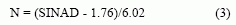
This equation is the definition for effective number of bits, or ENOB.
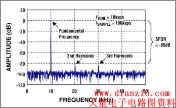
Figure 9. FFT plot reveals AC performance of an ADC.
Note that SINAD is a function of the input frequency. As frequency increases toward the Nyquist limit, SINAD decreases. If the specification in the data sheet is tested at low frequencies compared to the Nyquist frequency, you can bet the performance will be much worse near Nyquist. Look for an ENOB graph in the Typical Operating Characteristics of the data sheet. ENOB degrades with frequency primarily because THD gets increasingly worse as the input frequency increases. For example, with a SINAD minimum value of 68dB at the frequency of interest, you obtain an ENOB value of 11. Therefore, you have lost 1 bit of information due to the converter's noise and distortion performance. This means that your 12-bit converter can provide only 0.05% accuracy at best. Remember that INL is a DC spec; ENOB is the specification that tells about nonlinearities for AC signals.
SNR is the signal-to-noise ratio with the distortion components removed. SNR reveals where the noise floor of the converter is. There can be a steep decrease in SNR as a function of input frequency, which means the converter was not designed for frequencies near this point. One way to improve SNR is to oversample, which provides a processing gain. Oversampling is a method of lowering the noise floor of the converter by sampling at a rate much higher than the signal of interest. This spreads the noise out over a wider range in the frequency domain, thereby effectively reducing the noise at any one frequency bin. A 2X oversampling reduces the noise floor by 3dB.
SFDR is defined as the ratio of the RMS value of an input sine wave to the RMS value of the largest spur observed in the frequency domain using an FFT plot. It is typically expressed in dB. SFDR is important in certain communication applications that require maximizing the dynamic range of the ADC. Spurs prevent the ADC from converting small input signals, because the distortion component can be much larger than the signal of interest. This limits the dynamic range of the ADC. Note that a large spur in the frequency domain may not significantly affect the SNR, but will significantly affect the SFDR.
Final Thoughts
Returning to the ADC example, assume we are measuring DC-type signals and our ADC accepts bipolar input signals. We choose the B grade of the MAX1241, which has 1LSB DNL error, 1LSB INL error (0.0244%), 3LSB offset error (3/4096 = 0.0732%), and gain of 4LSB (0.0977%). Adding the errors, we obtain a total error of 0.1953%. We can calibrate out the offset and gain errors, dropping our error to 0.0244%. As long as our voltage-reference error is less than 0.075% - 0.024% = 0.051%, we are within the error budget. A 5ppm/°C drift of more than 50 degrees equates to a 0.025% drift error, with a 0.026% error budget remaining. For 12-bit performance, we need to have a voltage reference with a voltage-noise specification considerably less than 1LSB (which is 2.5V/4096 = 610µV peak-to-peak or 102µV RMS). The MAX6166 is a good choice with 5ppm/°C drift and 30µV RMS wideband voltage noise. It also has ample source and sink current capability to drive the ADC (and additional circuitry if needed). Note that the 30µV noise spec equates to 180µV peak-to-peak, which is one-third of an LSB at the 12-bit level and one-sixth of an LSB at the 11-bit level (which is what our system requirement actually is).
A quick check of the MAX1241 gain drift reveals a specification of 0.25ppm/°C or 12.5ppm over a 50°C temperature change, which is well within spec.
Now we have a viable solution that should prevent any hidden performance hiccups due to the specifications. Note for this example that we didn't address the AC performance at all. However, with your better understanding of the ADC specs and how they relate to the converter's performance, you will be armed with enough information to select the ADC that will give you the performance you need.
如果觉得
ADC中的ABC:理解ADC误差对系统性能的影响,The A这篇文章不错,可以推荐给朋友分享哦。
 温馨提示; 本站的资料全部免费下载,为方便下次找到本站记得将本站加入收藏夹哦,牢记网址http://www.dianzi6.com