6A RGB LED Driver Reference Design for a Portable Projector
6A RGB LED Driver Reference Design for a Portable Projector
Abstract: This is 6A step-down LED driver based on the MAX16821 device. This circuit drives a single LED. This application note includes the circuit specifications, circuit schematic, and circuit description and performance.
Introduction
This is a reference design for a 6A step-down LED driver for a portable projector. The reference design is based on the MAX16821, a PWM HB LED driver. This circuit drives a single LED; three MAX16821 devices are required to drive RGB LEDs.
LED Driver Specifications
- Input supply voltage (VIN): 10V to 15V
- Output voltage (VLED): 4.5V to 6V
- Output current (ILED): 1.5A to 6A with analog control
- Analog control voltage: 1.1V to 2.8V for 1.5A to 6A
- Maximum LED on duty cycle: 50%
- Maximum LED current rise/fall times: < 1µs
- Maximum LED current ripple: < 15% at 6A
Inputs
- VIN (J1 and J2 VIN+, J3 and J4 GND): 10V to 15V input power supply
- On/Off (J8): leave open or drive +5V to enable the driver. Short for disabling the board.
- PWM input (J7): dimming PWM input. Connect a PWM signal with 3V to 5V amplitude. The source should provide rise/fall times less than 500ns with a 300pF load so that the PWM input can drive Q1 and Q7. As output can rise/fall within 1µs, any PWM period three to four times higher than 1µs can be used.
- LED current control (J6): LED current adjust input. Apply 1.1V to 2.8V to adjust LED current from 1.5A to 5A.
Outputs
- LED+ (J9, J10): connect anode of LED.
- LED- (J11, J12): connect cathode of LED.
- Inductor current output (J5): provides a signal proportional to the LED current. The voltage at OUTV will be 135x the voltage across R9.
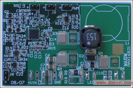
More detailed image (PDF, 2.23MB)
Figure 1. The LED driver board features the MAX16821.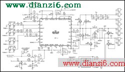
More detailed image (PDF, 2.63MB)
Figure 2. Schematic of the LED driver board.
Circuit Description
This LED driver steps down a 10V to 15V input supply voltage to drive a constant current to an LED with a 4.5V to 6V forward voltage. The MAX16821 PWM HB LED driver is used to implement the step-down converter. Since the average inductor current equals the LED current, the average inductor current can be controlled to drive a constant current to an LED. The switching frequency is set to 300kHz by R6 (200kΩ).
Two control loops are present: an inner current loop controls the inductor current based on the output of the outer voltage loop; the outer voltage loop programs the inner current loop to control the LED current. The outer voltage loop monitors the OUTV pin and the output of U1 to generate the EAOUT signal. That EAOUT signal controls the inner current loop and, thus, the inductor current.
Analog LED Current Control
An op amp, U1, takes an analog input from 1.1V to 2.8V and drives the SENSE+ input of the MAX16821 to adjust the LED current from 1.5A to 6A. When 6A is driven to the LED, the reference voltage and the resistive-dividers connected to U1 produce about 20mV (higher than the worst-case V
OL) at U1's output. A voltage of 2.8V at the analog control input produces this output voltage. When the LED current reaches 6A, the resistive-divider, comprised of R1 and R22, adds a fraction of current-sense signal at OUTV to the output of U1; R1 and R22 produce a voltage equal to the 100mV outer-loop reference at the SENSE+ input. Note that the OUTV signal is the amplified version of the current-sense signal across R9 and R18 with an amplification of 135V/V. As the voltage at the analog control input is reduced from 2.8V, the output of U1 increases linearly from 20mV. A higher voltage at the output of U1 takes the SENSE+ input to 100mV at a lower LED current. When the analog control input reduces to about 1.1V, the output of U1 increases to 80mV and the LED current reduces to 1.5A.
PWM Dimming
During the PWM off time, the MOSFET Q9 connected across the LED output is turned on, thus short-circuiting the LED. The LED current reduces to zero, depending on the turn-on time (much less than 1µs for this design) of Q1. Inductor current is maintained throughout the PWM off period. Q1 is turned off and the inductor current charges the output capacitor at the beginning of the PWM on time. Once the output voltage reaches the LED's cut-in voltage, the LED current starts to rise. The time required for the LED current to rise from 0A to the full value depends on several factors: the inductor current, the value of the output capacitor, and the change in the LED forward voltage from cut-in to full current. This reference design meets the < 1µs LED turn-on time specification
only when the LED current is set for 6A. The inductance value can be increased and the output capacitance reduced to achieve a fast LED turn-on at lower currents.
Feedback Compensation
Resistors R2 and R23 limit the high-frequency current-loop gain to compensate for subharmonic oscillations. A zero is placed in the current-loop transfer function much below the crossover frequency to ensure sufficient gain at low frequency and to enable the settling of the inductor current with low error. This zero is added using C1 and C19. Q1 and Q2 connect alternate RC networks for compensation during the PWM off and PWM on periods. This design maintains the charges in C1 and C19, and makes the PWM response much faster.
There is no output pole in the driver circuit's transfer function, as the inductor current is directly measured. The outer voltage loop thus reduces to a single-pole system with the voltage-error amplifier contributing the only pole within the frequency range that is considered. C21 and C22 reduce the outer-loop crossover frequency to one tenth of the current-loop crossover frequency to avoid any interaction between the two feedback loops. Q7 and Q10 retain the compensation capacitor charges, and allow the voltage-error-amplifier output to switch to the required value immediately when the PWM pulse changes state. Resistors R24 and R25 are used to avoid charging/discharging C21 and C22 due to charge injection when Q7 and Q10 change state.
LED Current Rise/Fall Times
This design requires the LED current to rise/fall within 1µs during PWM at a 6A LED current. This is enabled with a small output filter capacitor and a higher value inductor which meet the maximum ripple specification for the LED current. During PWM off, Q9 is turned on to circulate the programmed inductor current locally. If the LED current is set at 6A, then the inductor current is regulated at 6A by the MAX16821.When the output is turned on again, the inductor current charges the output capacitor, C8. The rate at which C8 is charged determines the LED current rise time; the value of C8 is calculated based on this. The fall time of LED current will be much less than 1µs because Q9 discharges C8 much faster.
Circuit Waveforms
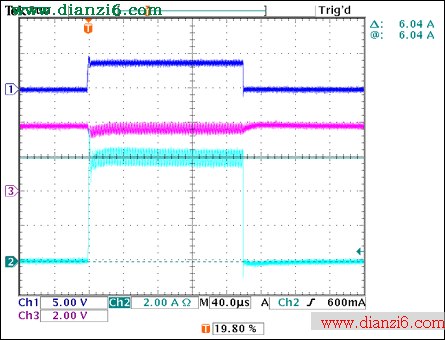 Figure 3. Test data for the reference design show the LED voltage (CH1), LED current (CH2), and OUTV voltage (CH3).
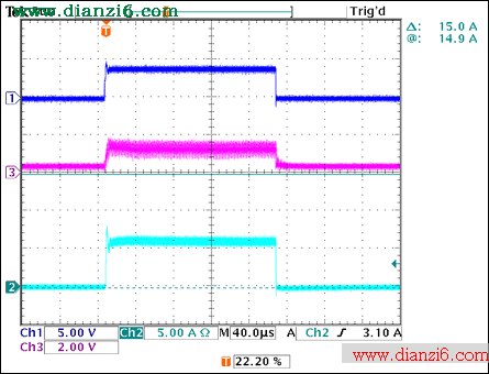 Figure 4. Test data show the LED voltage (CH1), LED current (CH2), and CLP voltage (CH3).
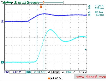 Figure 5. Data for the LED voltage (CH1) and LED current (CH2) rise time.
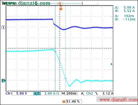 Figure 6. Test data for the LED voltage (CH1) and LED current (CH2) fall time.
Test Parameters
Temperature Measurements
- VIN: 10V
- IOUT: 6A
- TA: 25°C
- Board temperature: +50°C
- Q3, Q4, and Q9 case: +52°C
- U1 top: +47.5°C
- L1 core temperature: +75°C (L1 rated for 40°C rise above ambient at 5.8A)
Power-Up Procedure
- Connect a 0 to 20V, 5A power supply (PS1) to VIN+ and GND.
- Connect a 0 to 5V power supply (PS2) to J6 (V_CONTROL).
- Connect an LED rated for > 6A to LED+ and LED- with shortest possible leads to reduce inductance. If leads need to be long, then twisted-pair wires can be used.
- Keep J5 and J8 open.
- Turn on PS2 and apply 1.1V.
- Increase PS1 gradually to 10V. The LED will turn on with a 1.5A continuous current.
- Connect a 30% duty-cycle pulse with 3V to 5V amplitude to PWM. The LED current will turn on and off with the PWM signal.
- Increase PS2 from 1.1V to 2.8V. The LED current will rise from 1.5A to 6A during PWM on.
如果觉得
6A RGB LED Driver Reference Design for a Portable Projector这篇文章不错,可以推荐给朋友分享哦。
 温馨提示; 本站的资料全部免费下载,为方便下次找到本站记得将本站加入收藏夹哦,牢记网址http://www.dianzi6.com