mc14015参数资料(推荐) 下载
- 文件类型:
- 芯片设计资料下载,芯片设计
- 文件大小:
- 2.16 MB
- 下载次数:
- [288次]
- 日期:
- 09-20
- 解压密码:
- www.dianzi6.com
- Tag:
- 芯片设计,芯片设计资料下载 EFBA 参数 资料 推荐
- 运行平台:
- txt/doc/word/ppt/pdf 等
- 星级:
-

-

简介:
正文:
二极管保护所有投入
电源电压范围= 3.0直流电压至18日直流电压
逻辑边陇CClocked倒装陇CFlop设计 逻辑状态是无限期保留或者时钟水平过高或过低; 资料转移到输出只有在积极的去 边缘的时钟脉冲。
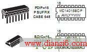
能够驱动双低陇Cpower的TTL负载或一低陇Cpow 肖特基的TTL负载的额定温度范围内工作。 The MC14015B dual 4¤Cbit static shift register is constructed wit MOS P¤Cchannel and N¤Cchannel enhancement mode devices in single monolithic structure. It consists of two identical, independent 4¤Cstate serial¤Cinput/parallel¤Coutput registers. Each register independent Clock and Reset inputs with a single serial Data input. The register states are type D master¤Cslave flip¤Cflops. Data is shift from one stage to the next during the positive¤Cgoing clock transition Each register can be cleared when a high level is applied on the Reset line. These complementary MOS shift registers find primary use in buffer storage and serial¤Cto¤Cparallel conversion where low pow dissipation and/or noise immunity is desired. ? Diode Protection on All Inputs ? Supply Voltage Range = 3.0 Vdc to 18 Vdc ? Logic Edge¤CClocked Flip¤CFlop Design Logic state is retained indefinitely with clock level either high or low; information is transferred to the output only on the positive going edge of the clock pulse. ? Capable of Driving Two Low¤Cpower TTL Loads or One Low¤Cpow Schottky TTL Load Over the Rated Temperature Range.
如果觉得《mc14015参数资料(推荐)》不错,可以推荐给好友哦。
正文:
二极管保护所有投入
电源电压范围= 3.0直流电压至18日直流电压
逻辑边陇CClocked倒装陇CFlop设计 逻辑状态是无限期保留或者时钟水平过高或过低; 资料转移到输出只有在积极的去 边缘的时钟脉冲。
能够驱动双低陇Cpower的TTL负载或一低陇Cpow 肖特基的TTL负载的额定温度范围内工作。 The MC14015B dual 4¤Cbit static shift register is constructed wit MOS P¤Cchannel and N¤Cchannel enhancement mode devices in single monolithic structure. It consists of two identical, independent 4¤Cstate serial¤Cinput/parallel¤Coutput registers. Each register independent Clock and Reset inputs with a single serial Data input. The register states are type D master¤Cslave flip¤Cflops. Data is shift from one stage to the next during the positive¤Cgoing clock transition Each register can be cleared when a high level is applied on the Reset line. These complementary MOS shift registers find primary use in buffer storage and serial¤Cto¤Cparallel conversion where low pow dissipation and/or noise immunity is desired. ? Diode Protection on All Inputs ? Supply Voltage Range = 3.0 Vdc to 18 Vdc ? Logic Edge¤CClocked Flip¤CFlop Design Logic state is retained indefinitely with clock level either high or low; information is transferred to the output only on the positive going edge of the clock pulse. ? Capable of Driving Two Low¤Cpower TTL Loads or One Low¤Cpow Schottky TTL Load Over the Rated Temperature Range.
如果觉得《mc14015参数资料(推荐)》不错,可以推荐给好友哦。
- 下载

- 进入下载地址列表
 温馨提示; 本站的资料全部免费下载,为方便下次找到本站记得将本站加入收藏夹哦,牢记网址http://www.dianzi6.com