热门关键字:
| 电路设计 单片机学习 PCB设计 电子制作 电工基础 电路基础 电子电路图 电脑技术 维修教程 手机数码 家电维修 电力技术 电气技术 |
| 电子基础 arm嵌入式 集成电路 模拟电子 电源管理 显示光电 楼宇控制 安防监控 控制电路 音响功放 单元电路 电子下载 维修资料下载 |
Reduced Termination Loss by Active Synthesis of Output Impedance |
Abstract: In high-speed transmission-line applications, it is important to match the output impedance of a line driver to the line. While this is achieved usually with a resistor, an active impedance synthesis has advantages. This application note describes how to use positive feedback around an op amp to create the desired output impedance. Equations and circuit examples are given for low-noise audio, and video op amps driving 50Ω to 600Ω loads. The Need for TerminationThe output impedance of a circuit is important in transmission line-driving applications. The transmission line impedance, which is determined by the physical geometry of the conductors and insulation, must be matched at both the send and receive ends in order to minimize degrading signal reflections. When the characteristic impedance is not correctly matched at the drive and the receiver ends, not all of the signal energy is delivered to the load. Some energy is reflected back and will distort (or sometimes, almost cancel) the forward signal to the load.RF engineers require accurate 50Ω terminations for their coaxial cables, video transmission engineers require accurate 75Ω terminations for their cables, and broadcast engineers require accurate 600Ω terminations for their audio circuits. Other standard termination values are 110Ω, 120Ω and 500Ω. The termination requirements are not confined to analog signals. Digital signals depend on correct line termination for accurate, high-speed transmission throughout a system. Passive Resistive TerminationThe usual method for achieving termination is to use a buffer amplifier with low output impedance, and add series resistance to the required value. This approach is simple, provided that the preceding buffer amplifier truly has a low output impedance across the band of interest.A serious disadvantage of the simple resistor approach is, however, the 6dB loss of signal between the buffer output and the terminated load. This results in a serious loss of signal headroom, particularly in single supply systems. Figure 1 shows a closed-loop buffer amplifier with a series resistance added outside the feedback loop to set the output impedance when measured looking back into the amplifier load terminal. 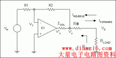 Figure 1. Simple passive termination. Note in Figure 1 that forward current into the load, IFORWARD, is determined by VO/RLOAD. Synthesised output impedance, ROUT, is determined by VO/IREVERSE, when VIN is zero. The understanding here is that the closed-loop output impedance of the op amp is low enough over a wide enough bandwidth to be ignored. Thus the chosen resistances set the output impedance. In Figure 1, RΘ is the series resistor that sets the impedance looking back into the output of IC1. RΘ = RLOAD = ROUT for correct back termination. The open-loop output resistance of the op amp is shown as ROOL. Voltage Gain is given by: 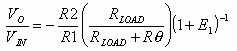 Error term is given by:  Output Impedance is given by: 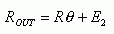 Error term is given by: 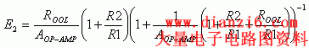 Errors due to finite open-loop gain (AOP-AMP) of the op amp are shown. Assuming infinite open-loop gain from an ideal op amp.  Assuming infinite open-loop gain from an ideal op amp. 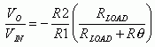 Figure 1 Advantage:
Active Synthesis of Output ImpedanceFortunately, a method exists to set output impedance and reduce the gain loss. The careful use of positive feedback around a voltage difference amplifier boosts a low-value output current-sensing resistor to the required final value.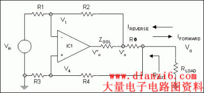 Figure 2. Single Op Amp active termination. Note in Figure 2 that forward current into the load, IFORWARD, is determined by VO / RLOAD. Synthesised output impedance ROUT is determined by VO/IREVERSE, when VIN is zero. Figure 2 shows a single op amp with both negative and positive feedback loops setting gain and output impedance. RΘ is placed in series with the load, and is used to sample the current into the load. Positive feedback through R3 and R4 is used to boost the effect of RΘ. For circuit stability, negative feedback must dominate the proceedings, and this fact limits the amount of boost available. The open-loop output resistance of the op amp is included to allow for the situation when ROOL becomes close in value to RΘ at high frequencies as the loop gain rolls off. Voltage Gain for Figure 2 is given by: 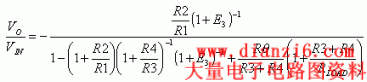 Error term is given by: 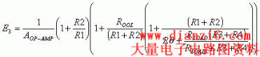 Output Impedance for Figure 2 is given by: 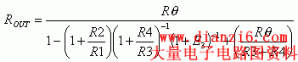 Errors due to finite open-loop gain of the op amp are shown. Note that the overall input-to-output signal path in Figure 2 is inverting. Assuming infinite open-loop gain from an ideal op amp, output impedance is: 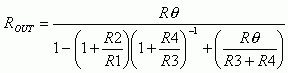 Generally, the term [RΘ / [R3 + R4]] is << [1 + R2 / R1][1 + R4 / R3]-1, so may be ignored.  Assuming infinite open-loop gain from an ideal op amp, voltage gain is: 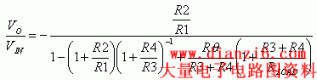 Rearranging the output impedance into the gain equation: 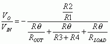 In general, RLOAD = ROUT for reverse-termination applications. Thus:  Figure 2 Advantages:
Measurement of Output ImpedanceThere are some simple ways to measure the impedance modulus looking back into the output terminals of the circuit. The measurement of the output impedance of the circuit under test is shown in Figure 3. The input to the circuit under test is grounded.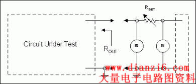 Figure 3. Measure output impedance. Perhaps the obvious approach in Figure 3a is to set the value of RSET at a particular frequency, so that |E2| is ½|E1|. The value shown on RSET is equal to ZOUT of the circuit under test. This is only true if ZOUT is purely resistive at the test frequency. Any reactive component will introduce large errors into this so called "6dB" method. A more accurate approach is to adjust RSET for |E2| 20dB less than |E1|. Then: |ROUT| = RSET / 9 Practically, RSET may be fixed at a value 10x the nominal impedance to be measured. The ratio of E1 and E2 then leads to the value of "ZOUT." If the ratio is made 40dB: |ROUT| is given by RSET / 99 Care needs to be exercised when using the 40dB ratio, as the source voltage could be greater than the breakdown of the circuit under test. This is relevant when low-voltage op amps are under consideration. A second method is to use a suitable network analyser. A third method, specific to active impedance boosting techniques, is to measure the voltage and phase directly across the current-sense resistor RΘ. From the voltage difference, the synthesised output impedance is given by: Referring to Figure 2. 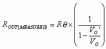 Referring to Figure 2, and taking into account the effect of R3 and R4 in parallel with the output. 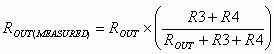 The incident or input drive voltage from the test source is VO (in Figure 2), and the reflected voltage from the op amp output is VO' (in Figure 2). A vector voltmeter can be used to extract both amplitude and phase difference. The ratio VO' / VO is further modified by Cos q. The big drawback of this method is the need to identify small voltage differences across RΘ in the presence of relatively large signal levels. DesignThe circuit shown in Figure 2 is chosen when a specified output resistance is required for a very low loss between amplifier and final output. RLOAD and ROUT are both known quantities. RΘ is chosen to be as small as possible, commensurate with overall circuit stability.By how much should RΘ be "boosted"? A practical upper limit is x10 (ie RΘ = 0.1 RLOAD). This will produce a termination loss of 0.83dB. A thorough analysis of each situation should be performed, but some of the variables, such as open-loop output resistance, are difficult to confirm from data sheet specifications. The higher the boost, the more positive feedback is applied, giving rise to reduced phase margins and increased closed-loop distortion. The final choice of "boost" will be a delicate compromise between termination loss and other closed-loop parameters. The operational amplifiers should be chosen to have unity-gain stability. Ensure that the time constant of the negative feedback loop dominates the overall loop control. This means that the positive feedback loop ideally should roll off before the negative feedback loop. Referring to Figure 2, the first-order time constant (TC) of the negative feedback loop is: 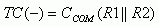 The time constant of the positive feedback loop is: 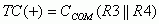 CCOM = Common mode capacitance at + and - inputs of the op-amp. Set TC(-) < TC(+). This assumes that the capacitance at the op-amp inputs is greater than the parasitic capacitance of the feedback loop resistors. In wideband situations it is appropriate to split each of R1-R4 into two equal value resistors to effectively halve the parasitic capacitance. If the circuit does not actually oscillate, there may be in-band response peaking. This can be checked by sweeping the circuit with a small signal (50mV to 100mV) sine wave to identify and plot the closed-loop frequency response (with load), and by correcting any in-band peaking by adjusting the feedback time constants. Example 1600Ω single ended audio cable active termination.Power supply = +5V Gain = 1 (0dB) ROUT = RLOAD = 600Ω. Chose termination loss = 1dB. The op-amp is chosen for its excellent distortion characteristics, bandwidth, and output drive capability. It is also unity-gain stable.  ROUT = RLOAD, and Gain = 1. 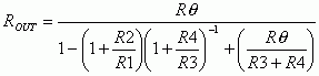 RLOAD = 600R for test purposes, and RΘ = 75R as nearest preferred value. RΘ = 0.125RLOAD. R2 = 0.25R1 Let R1 = 10k, then R2 = 2.5k. Use R2 = 2.4k + 100R. Then:  given that RΘ, and RLOAD = ROUT as shown above. This ratio provides the boost to RΘ. R4 = 0.428R3. Let R3 = 10k. Then R4 = 4.28k. Use R4 = 4.3k. 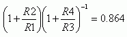 Figure 4. Example 1 (Power supply decoupling not shown for clarity). Table 1. Gain vs. Frequency [0dB = 137.5mVRMS]
Table 2. Voltage Difference Across RSET = 6.2kΩ (Fig3) 0dB = 486mVRMS
Calculated gain = -0.18dB with values shown above. Calculated output impedance = 572Ω. This value is determined by R3+R4 || ROUT reducing the calculated value. Example 250Ω single-ended active terminated broadband cable driver.Power supply = +5V. Gain = 1 (0dB). ROUT = RLOAD = 50Ω. Chose termination loss = 1dB. The op amp is chosen for its excellent distortion characteristics, bandwidth, and output drive capability. It is also unity-gain stable. For 1dB termination loss.  RLOAD = 50R for test purposes, and RΘ = 6.8R as nearest preferred value. RΘ = 0.136RLOAD. R2 = 0.272R1. Let R1=1k. Then R2=272R. Use R2=270R as nearest preferred value. Then: when RΘ and RLOAD = ROUT as shown above. This ratio provides the boost to RΘ. R4=0.472R3. Let R3=1k. Then R3 = 472R. Use R3=470R as nearest preferred. 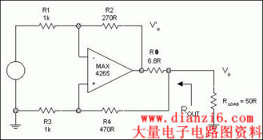 Figure 5. Example 2 (Power supply decoupling omitted for clarity). Table 3. Gain vs. Frequency 0dB = 70mVRMS
Table 4. Voltage Difference Across RSET = 510R (Fig3) 0dB = 225mVRMS
Calculated Gain = -0.63dB with values shown above, and taking into account additional 50Ω source resistance not included in R1. Calculated Output Impedance = 45.5Ω. This value is determined by R3 + R4 || ROUT reducing the calculated value. ConclusionThe careful application of positive feedback around a conventional voltage difference operational amplifier may be used to synthesise an output impedance higher than the usual value obtained from the application of negative feedback. This is useful in single-supply amplifier applications where the driving amplifier must drive the load from a known source impedance. A termination "gain" of some 5dB may be achieved compared to normal passive termination.Expressions have been developed to help gain an insight into the effects of open-loop gain and output impedance on the final closed-loop performance. Examples of the circuits have been built and demonstrate the ease of use of the circuits given. |
 温馨提示; 本站的资料全部免费下载,为方便下次找到本站记得将本站加入收藏夹哦,牢记网址http://www.dianzi6.com
|
此页提供Reduced Termination Loss by Ac电子电路基础,模拟电路基础, 电路基础参考。本站还有更多的电路基础相关资料分享。
Copyright© www.dianzi6.com Inc. All rights reserved 。 1 2 3 4 5 6 7 8 |
|