ШШУХЙиМќзжЃК
| Abstract: This document covers the three most popular topologies of voltage references. These include bandgap and buried zener topologies in three-terminal series voltage references and zener topologies in two-terminal shunt voltage references. Also demystified are the definitions of common voltage reference parameters. The first considerations in choosing a voltage reference are output voltage and initial accuracy. Often overlooked, however, are the various other data-sheet parameters that can assume major importance in specific applications. The following discussion of voltage-reference basics will help you better understand the performance parameters associated with the most common voltage-reference topologies: the two-terminal shunt and the three-terminal series designs. Two-Terminal (Shunt) ReferenceAs its name implies, the shunt reference operates in parallel with its load (Figure 1). It can be viewed as a voltage-controlled current sink in which the controlling voltage is applied to its input terminal. With no load applied, the shunt reference sinks just enough current so that the voltage drop across R1 produces the desired output voltage (VIN - IREFR1 = VREF). If, for example, VIN = 6.0V and the desired VREF is 5.0V, the reference IREF creates a 1.0V drop across R1. The reference then makes IREF adjustments as necessary to maintain 5.0V across its input.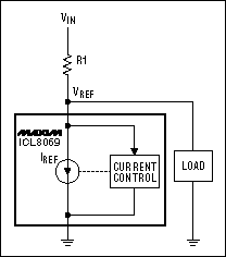 Figure 1. The shunt reference is connected in parallel with its load. Now apply a load to the reference. IREF no longer equals IR1, because load current (IL) produces part of the voltage drop across R1. The reference automatically reduces its sink current by the amount IL. Thus, the total current through R1 doesn't change (IREF + IL equals the original IR1). IR1 is shunted between reference and load, hence the name "shunt reference." A shunt reference regulates the output voltage by adjusting its sink current to oppose changes in load current. Three-Terminal (Series) ReferenceThe series reference operates in series with its load (Figure 2). It can be viewed as a voltage-controlled resistance in which VOUT controls an internal resistance between the reference's input and output terminals. A series reference regulates by creating a voltage drop between its input and output, which is equal to the product of the load current and the controlled internal resistance. With no load applied, the series reference draws a small amount of current (IQ) through the internal resistance (R) to drop a voltage between input and output necessary to produce the correct VOUT.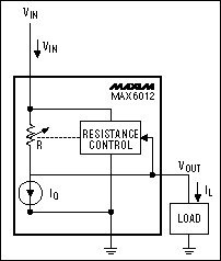 Figure 2. A series reference (its regulating part) is connected in series with its load. As load current increases, the reference maintains the desired output voltage by changing R as required to produce the correct drop between input and output. Applying Ohm's Law, one notes that to maintain a constant drop between input and output, R must decrease as IOUT increases. Parameter-Measurement Units for ReferencesThe units that specify parameters such as accuracy differ among the various manufacturers. For specifying accuracy, the units in common usage include parts per million (ppm), percentage (%), and voltage (V). All are acceptable, but to make "apples-to-apples" comparisons you must be able to convert one unit to any other. These relationships are clarified below.The most common means for stating reference accuracy is a percent of the nominal value, which isn't even a unit. It probably follows the convention for expressing tolerance on resistors, capacitors, and inductors. Typical percent-accuracy specifications for references are 1%, 1.5%, 2%, 5%, etc. Although percent accuracy is fine for comparing one reference with another, it does not provide specific information on how much the reference voltage deviates. What really matters is the variation in volts. To determine the voltage deviation of a reference specified in percent accuracy, you multiply the nominal output voltage of the reference by the percent accuracy and divide by 100. For example, a 2.5V reference accurate to ЁР1.5% has a deviation of Because the reference error can be above or below nominal, the total deviation is twice this value, or 75mV. The total output voltage variation equals the nominal voltage plus or minus the error voltage: Knowing these voltage limits for the reference gives you specific design boundaries for the circuitry supported by the reference. Another reference-accuracy unit found in data sheets is parts per million, more commonly abbreviated "ppm." This unit is typically used to specify temperature coefficients and other parameters that change very little under varying conditions. For a 2.5V reference, 1ppm is one-millionth of 2.5 volts, or 2.5 microvolts. If the reference is accurate to within 10ppm (extremely good for any reference), its output tolerance is as follows:
Converting this to voltage accuracy,
Converting to percent, Use of the term "bits" as a unit, as in "16-bit reference," is somewhat confusing. Does it represent an actual measurement of accuracy, or does it mean the reference is accurate enough for a 16-bit ADC? A 16-bit reference could be accurate to 1LSB or 2LSBs, so it cannot necessarily be considered sufficient for a 16-bit system. On the other hand, a reference "accurate to 16 bits" is specified with hard numbers. If the unit is specified by an actual measurement, then "accurate to 16 bits" is simply the value of the parameter divided by the claimed bit accuracy expressed in decimal form. For example, a 2.5V reference, claimed to be 16-bit accurate (another extremely accurate tolerance for any reference), should deviate by no more than the decimal equivalent of 16 bits: 216 = 65536. Therefore, 1 bit is 1/65536 of the total value. In this case, 2.5/65536 Ёж 38µV. If we assume 1-bit accuracy (ЁР 1LSB), the output voltage can be 1 bit higher or lower than nominal, i.e., ЁР38µV. Converting to voltage accuracy,
Converting to percent,
Typical Parameters of Importance for ReferencesInitial accuracy speaks for itself. If you take a part off the shelf, connect it in a test circuit, and measure the output voltage, the measured value should be within the initial-accuracy tolerance specified in the data sheet. This spec is usually for room temperature only, and it provides a starting point for most of the other specifications.Temperature coefficient is the deviation of reference output voltage due to a change in the ambient or package temperature. Depending on the device structure and the way its output voltage is trimmed during the initial calibration, this output-voltage deviation can be positive (increasing with increasing temperature) or negative (decreasing with increasing temperature). By analogy, consider a simple resistive voltage divider (Figure 3A). Voltage at the common point (VOUT) is a fraction of the applied voltage VIN, equal to the ratio of the values of the two resistors. Both resistors change with temperature by the same percentage, maintaining a constant ratio, so VOUT also remains constant. 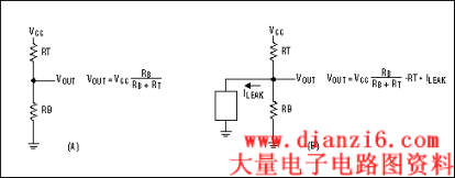 Figure 3. This simple resistor-divider analogy represents a voltage reference unloaded (A) and loaded (B). Note that current flowing through the resistors varies with the temperature and any leakage current from the common point of the divider (positive or negative) changes VOUT (Figure 3B). At room temperature, this change is usually compensated for by trimming one of the resistors (changing its value). However, if this variation of leakage current with temperature differs from the variation in divider current due to changes in the resistor values with temperature, the result is a change in VOUT with temperature. The VOUT change is called the temperature coefficient, or tempco. Although this analogy simplifies the more complex mechanism inside a reference circuit, it conveys the idea of a device tempco. Temperature hysteresis is the change in output voltage with a cycle of temperature variation. To measure, take a reference operating in a typical application, rated (as an example) for the extended operating temperature range (-40ЁуC to +85ЁуC), and record the output voltage at room temperature (+25ЁуC). Cool the reference to -40ЁуC, and then heat it to +25ЁуC. Measure and record the output voltage again. The difference in these measurements (if any) is the temperature hysteresis. Conversely, you can measure at +25ЁуC, heat the device to its maximum temperature (+85ЁуC), and then cool it back to +25ЁуC, measuring again. Any difference in these two room-temperature measurements also represents the temperature hysteresis. The deviation can be positive or negative. After many temperature cycles, one might deduce that the reference output voltage can be way off. Because temperature hysteresis is both positive and negative, however, the deviations resulting from a series of temperature cycles tend to cancel each other out, producing a final average output voltage very close to the nominal value. Line regulation, a measure of the change in output voltage due to a change in input voltage, is important if the input voltage changes while the reference is operating. Typical units are ppm/V and %/V. Line regulation is a DC parameter and is specified typically at DC. It measures the change in output voltage for two (or more) different DC input voltages, and it has little meaning if the input voltage varies rapidly, as for a voltage transient. In general, line regulation deteriorates inversely with the rate at which the line voltage changes. For applications likely to have line transients, reference-input capacitors are recommended to minimize the resulting variations. Load regulation is a measure of the change in output voltage due to a change in the reference load current. This parameter is important if the reference load current changes while the reference is operating. Again, load regulation is a DC parameter and is specified typically at DC. It measures the change in output voltage for two (or more) different DC load currents, and it has little meaning if the load current varies rapidly. In general, load regulation deteriorates inversely with the rate at which the load current changes. Output capacitors are recommended to stabilize the output voltage in applications subject to load-current transients. Typical units of measure are ppm/mA, %/mA, and percent change from no load to full load. Long-term drift (stability) is important if the reference must remain accurate for days, weeks, or years of continuous operation. It simply measures the variation in output voltage over a long period of time at some specified condition of steady-state operation. Long-term drift is a measure of the maximum and minimum output-voltage deviations over an extended time period, rather than a measure of deviation between "time A" and "time B." All other conditions (temperature, input voltage, load current, etc.) must be held constant if this measurement is to accurately reflect drift in the reference. Typical units are "ppm per 1000 hours." Supply current is self-descriptive, but consider these variations: For a series reference, the term "no-load current" is usually specified in the data sheet and often used interchangeably with the term "quiescent current." Because it designates the actual current drawn by an unloaded reference, no-load current does not specify the current drawn by that reference when loaded. Typical shunt references do not specify no-load current in the data sheet. Instead, they often list a minimum operating current (IMO). This parameter specifies the minimum current a reference must draw to maintain regulation. Note that a shunt reference must draw at least the minimum operating current under full-load conditions. Its series resistor (R1) must therefore accommodate the maximum load current plus the minimum operating current (Figure 4). In some applications, the minimum operating current (called "regulation current" in some data sheets) is disregarded, because it is so much smaller than the load current. 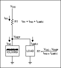 Figure 4. Current flow is the key for analyzing the operation of a shunt reference. Ground current: Often specified for a series reference, ground current measures the operating current at a given load. A series reference is in series with the load, so a measure of current flowing into the reference input yields the sum of load current and operating current. Ground current is often measured to determine the operating current for a series reference with load. Dropout voltage (VDO): very important in battery-operated equipment, applies only to the series reference. It is the minimum difference between input and output voltage that allows the reference to maintain its specified accuracy (VOUT + VDO = minimum input voltage). Battery voltage declines as the battery discharges, and to maximize useful life in the battery the reference must maintain an accurate output voltage while powered by the lowest-possible battery voltage. Thus, a lower dropout voltage allows continued operation at a lower battery voltage. Load capacitance: The ability of a reference to drive capacitive loads can be very important. Because typical references incorporate feedback control, their stability can be compromised by the zero introduced by a capacitive load; this can produce a large phase shift in the control loop that creates positive feedback at a particular frequency. Read the data sheet carefully for information on the range of load capacitance allowed. Some manufacturers refer to this limitation only in the text of the data sheet and not in the parameter tables. Noise: Although noise is apparent at a reference output, it is nonetheless often overlooked. A reference's noise, which is a random signal generated by active and passive devices inside the IC, affects its accuracy. For example, a 1mVp-p output noise voltage limits initial DC accuracy to no better than 1mV. For a 1.2V reference, this noise level alone limits initial accuracy to approximately 1%. Reference data sheets typically show noise in two frequency bands: low-frequency noise, ranging from 0.1Hz to 10Hz and specified in µVp-p, and wideband noise, ranging from 10Hz to 1kHz and specified in µVrms. Designating noise in two bands allows circuit designers to distinguish between wideband noise, which they can filter with practical capacitor values, and low-frequency noise, which they cannot. Also, if a capacitor large enough to filter the low-frequency noise were used, it is possible that the reference would be unstable with such a large capacitor placed at its output. AC line regulation: Although AC line regulation is not usually designated in a specification table, it directly influences the performance of the voltage reference. In most applications, the supply voltage to the reference has voltage spikes present. These spikes tend to be spread over a wide frequency range. The accuracy of the voltage reference is inversely proportional to the frequency of the input voltage variation. Because the AC line regulation is typically not specified, the reference data sheet should at least contain a graph showing the typical AC line regulation versus frequency. This graph would indicate the sensitivity of the reference to input system noise and could be used to determine the input filtering required. As the noise frequency increases, the input filtering must further reduce the input system noise in order for the reference to achieve its rated accuracy. AC load regulation/output impedance: The AC load regulation is another important parameter that is often left out of the specification table of a voltage reference. This parameter is important if the load current drawn from the reference is changing constantly. The accuracy of the reference is usually inversely proportional to the load variation frequency. A graph showing the AC load regulation or AC output impedance versus frequency should be contained in the reference data sheet. This graph should show what output filtering is required with the known output load variations in order to achieve the rated accuracy of the voltage reference. Line transient response: This parameter is typically shown as an oscilloscope screen shot displaying a step change in the input voltage and the resulting change and correction in the output voltage. This screen shot displays the recovery time of the reference in returning to a specified accuracy after such an event occurs. For this parameter, it is important to note the input and output capacitor values used. These capacitors have a tremendous effect on the performance of the reference. Load transient response/output settling time: This parameter is typically shown as an oscilloscope screen shot displaying a step change in the output current and the resulting change and correction in the output voltage. This screen shot displays the recovery time of the reference in returning to a specified accuracy after such an event occurs. For this parameter, it is important to note the input and output capacitor values used. These capacitors have a tremendous effect on the performance of the reference. Turn-on/turn-off settling time: The turn-on settling time is a measure of how quickly the output voltage of the reference stabilizes after an initial power-up. The output only needs to be stable and may not necessarily have reached the specified accuracy of the reference. Typically, this parameter is specified with an output voltage error greater than the specified accuracy, and it should always be given in the conditions of the parameter. This parameter is highly dependent on the input and output capacitor values used and the load applied to the reference. Turn-off time, on the other hand, is a simple measure of how long it takes for the output voltage of the reference to reach virtually zero volts. Likewise, this parameter is highly dependent on the input and output capacitor values used and the load applied to the reference. ConclusionVoltage references are often chosen in haste. Before making a decision, the designer will look at the price, the initial accuracy highlighted on the data sheet, and frequently nothing else. Make sure that you compare apples to apples when comparing references. When evaluating a specification listed on several data sheets, be sure that all are expressed in the same units. Determine what parameters are important for your application, and look beyond the initial-accuracy specifications.AppendixPopular Voltage-Reference TypesTwo-Terminal Shunt or Zener ReferenceA zener reference is based on the zener principle, in which the current in a reverse-biased diode begins to flow at a certain voltage threshold and then increases dramatically with an increase in voltage. A resistor in series with the diode establishes a constant current, allowing the zener to achieve a stable reference voltage. The zener reference behaves like a typical shunt or two-terminal reference. It can also be used as a voltage clamp.
Three-Terminal Series and Buried (Subsurface) Zener References
Three-Terminal Series (Bandgap) Reference Making a compromise between cost and outstanding performance (low-noise operation and accuracy), the bandgap reference has become one of the most popular voltage references available. It compensates for the effect of temperature by subtracting the negative-tempco voltage of a forward-biased base-emitter junction from a positive-tempco PTAT (proportional to absolute temperature) voltage. The PTAT voltage is generated by measuring and amplifying the voltage difference between two forward-biased diode junctions.
A similar article appeared in the April 2000 issue of EDN |
 ЮТмАЬсЪО; БОеОЕФзЪСЯШЋВПУтЗбЯТдиЃЌЮЊЗНБуЯТДЮевЕНБОеОМЧЕУНЋБОеОМгШыЪеВиМаХЖЃЌРЮМЧЭјжЗhttp://www.dianzi6.com
|
ДЫвГЬсЙЉUnderstanding Voltage-ReferencФЃФтЕчзгММЪѕЛљДЁ,ФЃФтЕчзгЕчТЗ, ФЃФтЕчзгММЪѕВЮПМЁЃБОеОЛЙгаИќЖрЕФФЃФтЕчзгММЪѕЯрЙизЪСЯЗжЯэЁЃ
Copyright© www.dianzi6.com Inc. All rights reserved ЁЃ 1 2 3 4 5 6 7 8 |
|